DDR3 Layout Guidelines: Essential Tips for PCB Design China a1 a2 sodimm ddr4 pcb layout guidelines ddr3 ram pcb design 2.0mm ...
If you are looking for Pcb Design Tips at Marjorie Hiller blog you've came to the right place. We have 25 Images about Pcb Design Tips at Marjorie Hiller blog like Complete Guide to PCB Layout Design: Tips, Basics, & Guidelines, Rf Pcb Design Guidelines Outlet Clearance | brunofuga.adv.br and also An520 DDR3 SDRAM Memory Interface Termination and Layout Guidelines. Here you go:
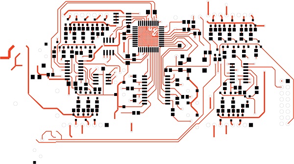
Pcb Design Tips At Marjorie Hiller Blog
 storage.googleapis.com
Pcb Design Tips at Marjorie Hiller blog
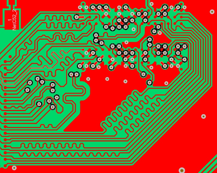
PCB Design Rules And Tips
 www.6pcb.com
PCB Design Rules and Tips
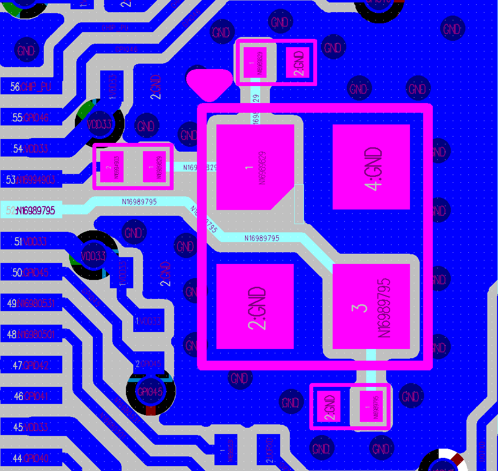
Grounding Pcb Crystal Layout Electrical Engineering S - Vrogue.co
 www.vrogue.co
Grounding Pcb Crystal Layout Electrical Engineering S - vrogue.co
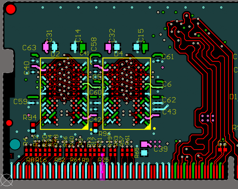
Top 5 Pcb Design Guidelines In Electronics Industry 2 - Vrogue.co
 www.vrogue.co
Top 5 Pcb Design Guidelines In Electronics Industry 2 - vrogue.co
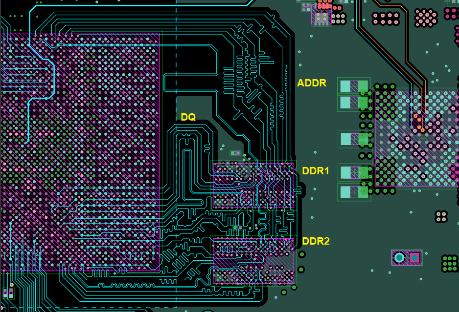
(PDF) DDR2/DDR3 Low-Cost PCB Design Guidelines For Artix-7 · The
 dokumen.tips
(PDF) DDR2/DDR3 Low-Cost PCB Design Guidelines for Artix-7 ... · The ...
What Is High Speed PCB Design - Guidelines And Best Practice Tips - IBE
 www.pcbaaa.com
What is high speed PCB design - guidelines and best practice tips - IBE ...
(PDF) Board Design Layout Guidelines; External Memory … · Introduce The
 dokumen.tips
(PDF) Board Design Layout Guidelines; External Memory … · introduce the ...
PCB Routing Guidelines For DDR4 Memory Devices And Impedance | Blog
 resources.altium.com
PCB Routing Guidelines for DDR4 Memory Devices and Impedance | Blog ...
PCB Layout Guidelines And Considerations
 www.microcontrollertips.com
PCB layout guidelines and considerations
18 PCB Layout Tips For Improving Your PCB Design And Reducing
 camptechii.com
18 PCB Layout Tips for Improving Your PCB Design and Reducing ...
PCB Design Guidelines For EMI EMC - RayMing PCB
 www.raypcb.com
PCB Design Guidelines For EMI EMC - RayMing PCB
Complete Guide To PCB Layout Design: Tips, Basics, & Guidelines
 sfxpcb.com
Complete Guide to PCB Layout Design: Tips, Basics, & Guidelines
Pcb Routing Guidelines - Design Talk
 design.udlvirtual.edu.pe
Pcb Routing Guidelines - Design Talk
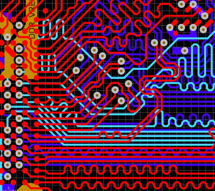
DDR, DDR2 And DDR3 – PCB Layout Examples
 www.fedevel.com
DDR, DDR2 and DDR3 – PCB layout examples
China A1 A2 Sodimm Ddr4 Pcb Layout Guidelines Ddr3 Ram Pcb Design 2.0mm
 www.chinax.com
China A1 A2 Sodimm Ddr4 Pcb Layout Guidelines Ddr3 Ram Pcb Design 2.0mm ...
Getting Started With RF PCB Layout Guidelines
 www.hemeixinpcb.com
Getting Started With RF PCB Layout Guidelines
High Speed Pcb Layout Guidelines - Design Talk
 design.udlvirtual.edu.pe
High Speed Pcb Layout Guidelines - Design Talk
Power Supply PCB Design Guidelines For Manufacturing - VSE
 www.vse.com
Power Supply PCB Design Guidelines for Manufacturing - VSE
An520 DDR3 SDRAM Memory Interface Termination And Layout Guidelines
 www.scribd.com
An520 DDR3 SDRAM Memory Interface Termination and Layout Guidelines ...
Rf Pcb Design Guidelines Outlet Clearance | Brunofuga.adv.br
 brunofuga.adv.br
Rf Pcb Design Guidelines Outlet Clearance | brunofuga.adv.br
PCB Layout Guidelines For High Speed Applications - HardwareBee
 hardwarebee.com
PCB Layout Guidelines For High Speed Applications - HardwareBee
How To Design Your Own PCB – From Basic Layout Tips – PCB HERO
 www.pcb-hero.com
How to Design Your Own PCB – From Basic Layout Tips – PCB HERO
Main Design Guidelines & Layout Rules On High Speed Printed Circuit
 www.integrasources.com
Main Design Guidelines & Layout Rules on High Speed Printed Circuit ...
Pcb Design Guidelines Mechanical Layer Eurocircuits Eurocircuits Images
 www.tpsearchtool.com
Pcb Design Guidelines Mechanical Layer Eurocircuits Eurocircuits Images
Main Design Guidelines & Layout Rules On High Speed PCB
 www.integrasources.com
Main Design Guidelines & Layout Rules on High Speed PCB
What is high speed pcb design. Main design guidelines & layout rules on high speed printed circuit. How to design your own pcb – from basic layout tips – pcb hero